

Department of Engineering Physics
Condensed matter physics Surfaces, interfaces and thin films Electronic materials and components Semiconductor fabrication and packaging Physics Experimental methods and instrumentation Electronic properties of solids Semiconductors Microelectronics Energy conversion and distribution Photonic devices and networks
Research interests and affiliations
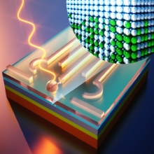
Our research is interdisciplinary encompassing fundamental scientific and technological activities in nanoscience and nanotechnology with focus on materials physics and engineering. The primary objective of our activities has been the development of processes for controlled nanoscale fabrication and manipulation of integrative and flexible semiconductor systems with actual or potential impact on electronics, photonics, optoelectronics, environmentally friendly energy conversion, and bio-integrated technologies. Particularly, we have been developing and employing unique combinations of nanofabrication and integration tools to enable a variety of novel complex and nanostructured materials thereby generating building blocks for scalable, high-performance, and multifunctional devices.
For more details, visit our web page: http://www.polymtl.ca/nhl/en/
- Lassonde Deeptech Institute, Scientific director
- Institut de l'énergie Trottier (IET), Member
- 2000 MATERIALS SCIENCE AND TECHNOLOGY
- 2002 Materials processing/fabrication
- 2009 Semiconductors
- 2010 Thin films/interfaces
- 2014 Crystals
- 3300 CONDENSED MATTERPHYSICS
- 3303 Surfaces, interfaces and thin films
- 3402 Surface and interfacial chemistry
- 3407 Crystallography - physical chemistry
Publications

Teaching
PHS2109: Cristallographie
PHS8302: Dispositifs Électroniques
PHS6910: Séminaires de Génie Physique
PHS2108: Mécanique Quantique I
PHS2114: Science et Génie des Matériaux
Supervision at Polytechnique
IN PROGRESS
-
Post-doctoral fellowship (6)
-
Assali, Simone. Group IV Infrared Materials and Devices.
-
Bayram, Sirine. Metal-free plasmonics.
-
Jendi, Zeina. Modeling of semiconductor structures and devices for energy applications.
-
Mukherjee, Samik. Growth and characterization of group IV semiconductor quantum structures.
-
Phan, Duy-Thach. 2D materials and sensors.
-
Waller, Olga. Growth and in situ Characterization of New 2D Materials.
-
-
Ph.D. (2)
-
Kumar, Aashish. Fundamentals of non-equilibrium group IV epitaxy.
-
Luo, Lu. Tensile strained germanium optoelectronic devices.
-
COMPLETED
-
Ph.D. Thesis (8)
- Lemieux-Leduc, C. (2025). Integration of Germanium-Tin Membranes for Mid-Infrared Silicon Photonics [Ph.D. thesis, Polytechnique Montréal].
- Del Vecchio, P. (2024). Dynamics and Spin-Orbit Coupling Properties of Light Holes Confined in Group-IV Semiconductor Heterostructures [Ph.D. thesis, Polytechnique Montréal].
- Luo, L. (2024). Ge/Ge1−xSnx Group IV Nanowires for Mid-Wave Infrared Optoelectronics [Ph.D. thesis, Polytechnique Montréal].
- Attiaoui, A. (2023). Optical Behavior of Group-IV Semiconductors in Relation to Atomic Interfacial Disorder, Quantum Confinement, and Fano Resonance [Ph.D. thesis, Polytechnique Montréal].
- Nicolas, J. (2022). Ingénierie de contrainte et stabilité des hétérostructures épitaxiales de Ge1-xSnx [Ph.D. thesis, Polytechnique Montréal].
- Fortin-Deschênes, M. (2020). Real-Time and Atomic-Level Studies of the Growth, Phase Transformations and Stability of Two-Dimensional Pnictogens [Ph.D. thesis, Polytechnique Montréal].
- Chagnon, D. (2018). Encapsulation hermétique de microbolomètres pour caméras infrarouges : optimisation et études in situ de l'instabilité des interfaces [Ph.D. thesis, École Polytechnique de Montréal].
- Mukherjee, S. (2017). Isotope Engineering and Lattice Disorder in Group IV Nanoscale and Quantum Semiconductors [Ph.D. thesis, École Polytechnique de Montréal].
- Lemieux-Leduc, C. (2025). Integration of Germanium-Tin Membranes for Mid-Infrared Silicon Photonics [Ph.D. thesis, Polytechnique Montréal].
-
Master's Thesis (13)
- Montpetit, L. (2025). Contact Interface Engineering and Thermal Stability of Direct-Conversion CdZnTe X-Ray Detectors [Master's thesis, Polytechnique Montréal].
- Nadal, G. (2025). La sonde atomique assistée par laser à large champ de vision : traitement de données tomographiques et analyses cristallographiques [Master's thesis, Polytechnique Montréal].
- Bellemare, C. (2024). La conductivité intrinsèque des semi-conducteurs Ge1−xSnx hors équilibre [Master's thesis, Polytechnique Montréal].
- Chane Kai Shing, R. (2024). Magnétophotoluminescence des semi-conducteurs Ge1−xSnx, facteur g∗ et décalage diamagnétique [Master's thesis, Polytechnique Montréal].
- Fettu, G. (2022). Mid-Infrared Optical Spin Injection and Coherent Control [Master's thesis, Polytechnique Montréal].
- Gendron-Paul, M. (2022). Magnéto-photoluminescence des alliages de GeSn : conception d'un montage et mesures préliminaires [Master's thesis, Polytechnique Montréal].
- Daligou, G. T. E. G. (2021). Silicon-Integrated GeSn Mid-Infrared Emitters : Theoretical Modeling and Device Demonstration [Master's thesis, Polytechnique Montréal].
- Abdi, S. (2020). Towards Ultra-Low Specific Contact Resistance On High Sn-Content GeSn For Mid-Infrared Optoelectronics [Master's thesis, Polytechnique Montréal].
- Groell, L. (2020). Passivation de la surface du GeSn pour le développement de l'optoélectronique intégrée opérant dans l'infrarouge moyen [Master's thesis, Polytechnique Montréal].
- Bouthillier, É. (2019). Non-Equilibrium Germanium-Tin Microstructures for Silicon-Compatible Mid-Infrared Photonics [Master's thesis, Polytechnique Montréal].
- Attiaoui, A. (2018). Non-Equilibrium SiGeSn Group IV Heterostructures and Nanowires for Integrated Mid-Infrared Photonics [Master's thesis, École Polytechnique de Montréal].
- Abboud, Z. (2016). In Situ Studies of Volatile Molecules Trapping in Zirconium Alloy-Based Non-Evaporable Getter [Master's thesis, École Polytechnique de Montréal].
- Fournier-Lupien, J.-H. (2015). Les alliages germanium-étain et silicium-germanium-étain: croissance, propriétés structurales et stabilité thermique [Master's thesis, École Polytechnique de Montréal].
- Montpetit, L. (2025). Contact Interface Engineering and Thermal Stability of Direct-Conversion CdZnTe X-Ray Detectors [Master's thesis, Polytechnique Montréal].
News about Oussama Moutanabbir


Press review about Oussama Moutanabbir


