
Blogue
A compact camera that sees through snow and fog

Professor Moutanabbir's team is designing semiconductors that make "vision" possible in the SWIR and MWIR infrared ranges of the electromagnetic spectrum - where use is difficult, owing to less-suitable tools currently available. (Credit: Nano and Quantum Semiconductors Laboratory)
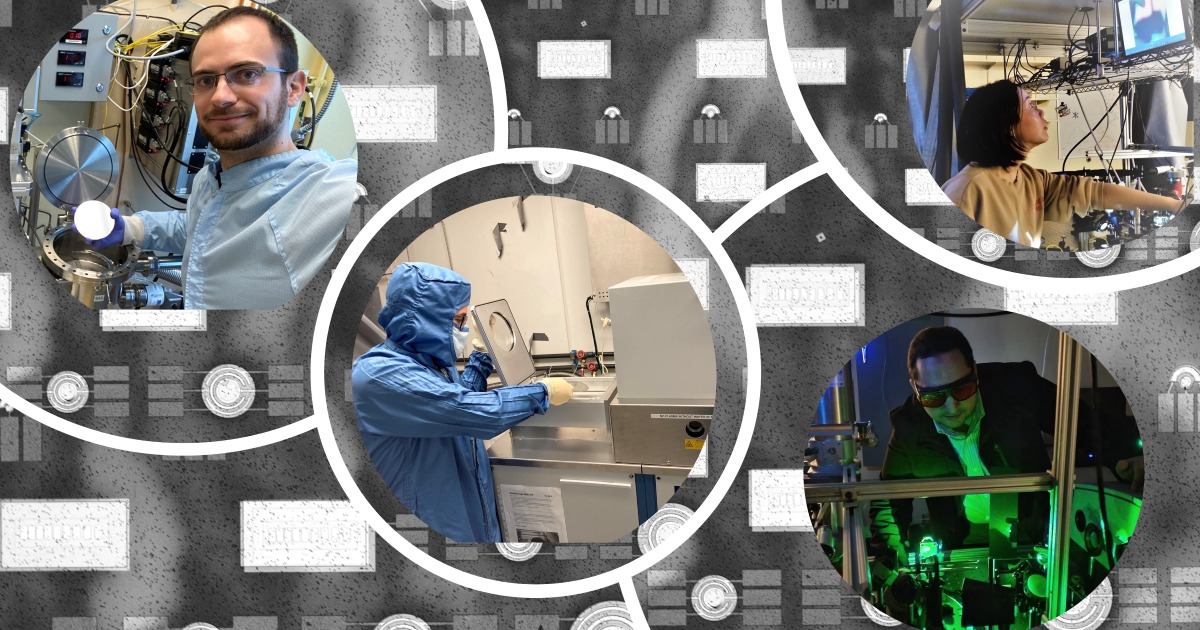
In his laboratory at Polytechnique Montréal, Professor Oussama Moutanabbir's team is developing a type of bionic vision: an in-house created photodetector made of semiconductors integrated into silicon chips. It could soon impact various technologies, including autonomous vehicle navigation systems, optical and data communication, thermophotovoltaics, and night vision cameras. It's a device that literally sees… through snow and fog!
When a snowstorm blusters in or fog rolls in, navigation systems still have a hard time finding their way around. The problem is particularly acute in autonomous vehicles and aviation, where drone, airplane, or helicopter pilots must navigate in extreme weather conditions.
 Professor Oussama Moutanabbir (Photo : Polytechnique Montréal)
|
There are existing infrared detection and imaging technologies that can in principle get around this problem, but the caveat "in principle" really applies here. In reality, these technologies are still far from being widely adopted. In fact, these cameras can cost well over $10,000 - and that's just one stumbling point. The other issue is size, the devices can be large, because they need a cryogenic system – something that hinders their use in civilian applications, in addition to imposing additional maintenance costs.
These difficulties could soon be a thing of the past, thanks to sensors developed by Full Professor Oussama Moutanabbir (Department of Physical Engineering) and his team at Polytechnique Montréal. By producing semiconductors sensitive to a specific infrared range, which are also compatible with silicon manufacturing processes, his group has been developing a cost-effective, compact, infrared camera capable of seeing what the human eye cannot!
The group has been working on this technology for years, thanks in part to support from the Innovation for Defence Excellence and Security program from Canada National defense's Innovation for Defence Excellence and Security program, Canada foundation for innovation (FCI), and PRIMA Quebec. The group recently reached key milestones by demonstrating the room-temperature efficiency of silicon-integrated photodetectors with a high bandwidth sufficient to realize spectroscopic photodetection applications. These results have just been published in two articles in ACS Photonics magazine, entitled: “High-Bandwidth Extended-SWIR GeSn Photodetectors on Silicon Achieving Ultrafast Broadband Spectroscopic Response” and “Extended-SWIR Photodetection in All-Group IV" Core/Shell Nanowires.” Both articles were first-authored by post-doctoral researcher Mahmoud R.M. Atalla, and PhD candidate Lu Luoz, respectively.
Seeing Infrared with a New Eye
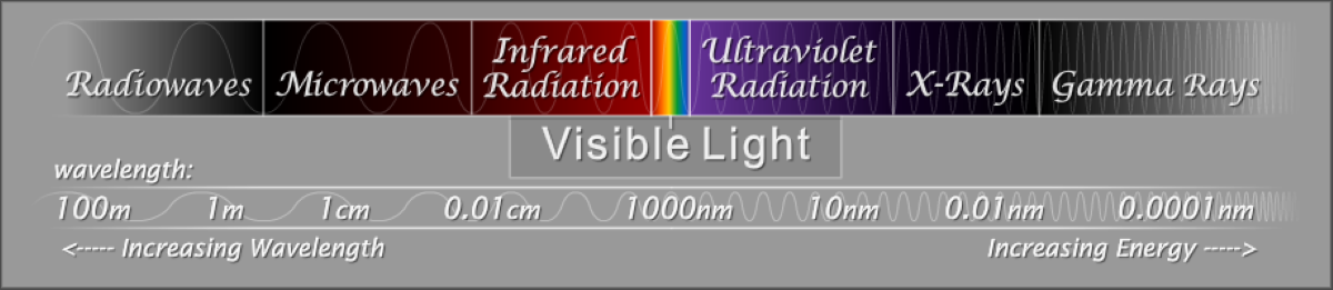 Infrared (IR) radiation ranges from 0.75 micrometres to 1000 micrometres. (Credit : Foumart, licence CC BY-SA 3.0)
I can hear you pondering this very question right now: "But infrared sight, isn't that already possible?" Yes.... and no.
The part of the electromagnetic spectrum that corresponds to infrared light is vast, and ranges from wavelengths of 0.75 micrometers to about 1000 micrometers. Thermal cameras that capture the heat given off by our bodies targets wavelengths ranging from 8 to 12 micrometers. Professor Moutanabbir's team is interested in the spectrum range that sits between 1.7 micrometers and 8 micrometers, a sub-region that essentially corresponds to short-wave infrared (SWIR) and mid-wave infrared (MWIR).
"The idea is not to detect heat radiation," explains the researcher from the Department of Physical Engineering. "Our sensor detects the light reflected by an object when it is illuminated by the light emitted at these wavelengths. It works like our eye or conventional cameras, but with a different kind of light. This light is invisible to our eyes, but actually, is abundant in our environment at night – it just needs to be detected."
The photodetector targets short- and mid-infrared wavelengths, solving the problem of visible light that's easily blocked by snow, ice, or fog. SWIR and MWIR wavelengths are able to see through these metrological phenomena. As a result, cameras based on this technology could see through a curtain of snow or fog, all without difficulty.
Spectrometry tools using these sensors could also be used to detect biochemical substances in the environment, as many molecules offer "spectroscopic signatures" in this range of the electromagnetic spectrum. The team at Polytechnique Montréal is also pursuing this line of development.
Thin layers... of germanium and tin |
|
If the sensors developed by the Polytechnique Montréal lab are different from the SWIR and MWIR technologies that already exist, it’s because they rely on a new family of semiconductors based on germanium and tin. Eventually, this technology could be integrated into LIDARs and navigation systems for autonomous vehicles. It could also be used in optical and data communication chips, and used in night vision cameras, or to detect specific chemical or biological agents by on-chip spectroscopy. It’s also envisaged to incorporate these sensors in thermophotovoltaic cells to harvest and convert residual heat emitted by various sources that exceed 500 degrees Celsius, into electricity. All this, for a tiny fraction of the cost of current technologies, according to the Professor who also holds the Canada Research Chair in Nanoscale and Quantum Semiconductors. "The fact that this technology is cost-effective to manufacture, and that it works at room temperature paves the way for all sorts of possibilities," Moutanabbir notes. The Professor also adds that this technological development is all the more interesting because we already have the expertise and technologies needed to develop this type of semiconductor in Québec. "There’s an international race happening to develop this type of technology, and we’re fortunate to be among the leaders," he adds. |
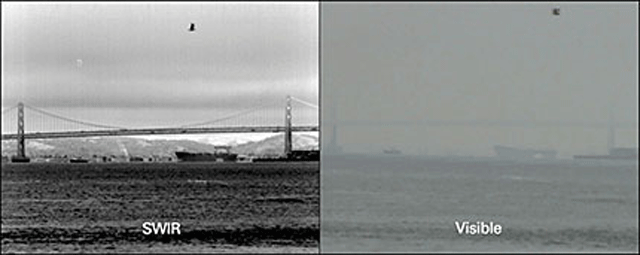 SWIR type camera technology - based on InGaAs – make it possible to see through fog. However, right now, cameras are still too prohibitively expensive to permit their large-scale use. (Credit : Sensors Unlimited)

Comments
Commenter
* champs obligatoire