

 Materials able to heal damage caused by external agents are highly desirable for applications in the electronics, biomedical, automotive and aerospace fields. The healing can be autonomic or non-autonomic, depending on whether or not an external stimulation is required. In particular, self-healing electronic materials can find applications in wearables, stretchable and bendable electronics, as well as in artificial electronic skin. The major challenges for self-healing electronic materials is to combine fast and reproducible healing characteristics, high conductivity, facile processing and, in the caseof applications for electronic skin, biocompatibility.
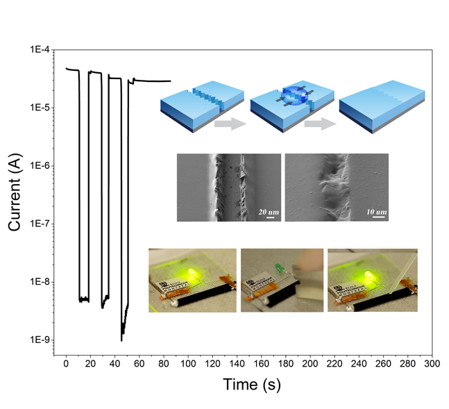
Our group reported the first observation of healable conducting polymer (PEDOT:PSS) films with an electrical conductivity as high as 500 S/cm. We observed electrical healing of pure PEDOT:PSS film after damage by simply covering the damaged area of the films with a droplet of water. The healing process takes place within an extremely short time (about 150 milliseconds) and enables complete restoration of the initial film conductivity, even after multiple damages. Significantly, PEDOT:PSS films wet with water behave as self-healing conductors: the current flow in the film is totally insensitive to external damage. The rapid electrical healing, combined with high conductivity and biocompatibility, places PEDOT:PSS in a highly competitive position among electrically healablematerials for applications in large-area self-healable electronics and electronic skin.
 Stretchable electronic devices, based on materials combining high electrical conductivity with mechanical elasticity, are of great interest for applications in wearable electronics and bioelectronics. They can be placed on textiles, three dimensional objects and soft biological tissues such as skin, heart, brain and muscles to monitor electrical and mechanical signals as well as body conditions.
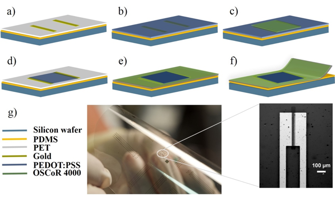
The large majority of stretchable electronic devices are currently fabricated on the organosilicon compound polydimethylsiloxane (PDMS). PDMS offers a number of unique and attractive features,such as optical transparency, biocompatibility, ease of process and a moderate elastic modulus, which permits conformable surface coverage of a wide variety of surfaces. The key steps forthe fabrication of high-resolution stretchable electronic devices (e.g., transistors) on PDMS are the patterning of the metallic contacts and the electroactive material.
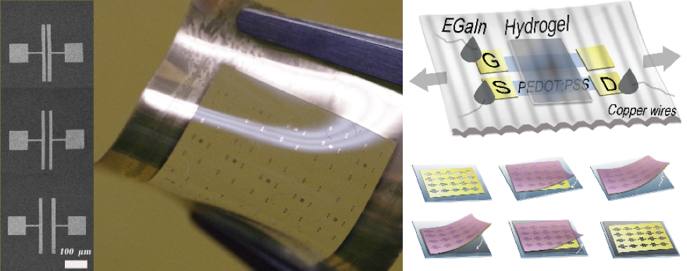
In our group we use high-fidelity processes to pattern both metal electrodes and organic electroactive materials on PDMS with high resolution. Metal electrodes, with channel length as short as 5 μm, were realized using Parylene transfer patterning, whereas the organic electroactive material was patterned by orthogonal photolithography. By taking advantage of those two patterning techniques and of a “cut and paste” hydrogel as stretchable electrolyte, we demonstrated fully stretchable organic electrochemical transistors (OECTs). The biocompatibility of all device components make our technology viable for in vivo bioelectronics.
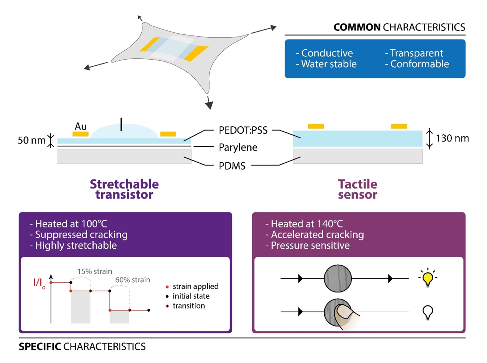
More recently, we reported strain-insensitive stretchable OECTs on polydimethylsiloxane (PDMS) substrates, fabricated with conventional technologies, without pre-stretching the substrates. Our OECTs maintain similar performance up to 30% strain (the maximum strain the human skin can tolerate). The stretchability is maximized by fine-tuning the composition, reducing the thicknesses and decreasing the baking temperature of PEDOT:PSS films. By interposing a thin parylene layer between the PDMS substrate and the PEDOT:PSS film, we were able to improve the ON/OFF ratio and the transconductance of the devices to levels comparable to OECTs on rigid substrates. We also demonstrate PEDOT:PSS films with thicker thicknesses or baked at higher temperatures, which are not ideal for developing stretchable OECTs due to their limited stretchability, can be used as transparent pressure sensors.
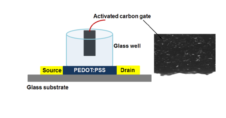
Organic electroactive materials are increasingly used to produce flexible, low-cost and easily processable electronic devices, such as organic light-emitting diodes, transistors and photovoltaic cells. Alongside these well-established applications, organic electroactive materials have recently been introduced in bioelectronics, the implementation between electronics and biology. The unique properties of organic electroactive materials, that make them ideal for application in bioelectronics, are their softness, flexibility and ability to translate electronic signals into ionic bio signals and vice versa. Examples of organic bioelectronic devices are sensors based on organic electrochemical transistors (OECTs) and conducting polymer electrodes for monitoring and stimulation.
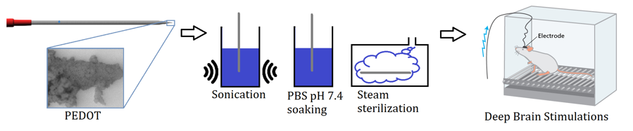
In our group we study the electropolymerization of PEDOT on platinum-iridium (PtIr) microelectrodes for deep brain stimulation and recording and on stainless steel electrodes for electromyography (EMG). To optimize the adhesion of PEDOT to the metal electrodes, we investigated several solvents. The adhesion of the coatings to the substrate and their electrochemical stability was tested through sonication, prolonged immersion in phosphate buffer solution, sterilization by autoclaving and electrical pulsing. Adhesion and electrochemical stability were evaluated using cyclic voltammetry (CV) in phosphate buffer saline and potentioelectrochemical impedance spectroscopy (EIS). PtIr stimulating microelectrodes coated with PEDOT:BF4 have been implanted in the brains of two rats, which were electrically stimulated daily up to 7 and 15 days. The impedance of the electrodes was measured in vivo before and after every stimulation. EMG electrodes are currently implanted in mice.
 Organic materials are in general incompatible with photolithography since they are highly soluble in organic solvents and can be damaged by direct contact with photoresists, developers and removers. In our laboratory we take advantage of an innovative process, where photoresists, developers and removers are based on fluorine chemistry. Fluorinated materials are immiscible in both polar and nonpolar solvents and are completely non-interacting with organic electroactive materials, which will not be damaged during the process. Alternatively, device fabrication is achieved using another patterning technique, where a sacrificial layer of the polymer Parylene C is used to avoid the contact between the organic electroactive material and the chemicals used in photolithography.
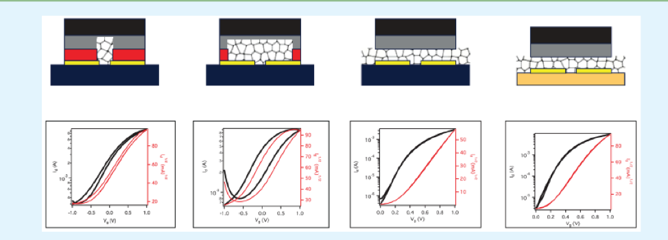 Metal oxides constitute a class of materials whose properties cover the entire range from insulators to semiconductors to metals. Most metal oxides are abundant and accessible at moderate cost. Metal oxides are widely investigated as channel materials in transistors, including electrolyte-gated transistors, where the charge carrier density can be modulated by orders of magnitude upon application of relatively low electrical bias (below -2 V). Electrolyte gating offers the opportunity to envisage new applications in flexible and printed electronics as well as to improve our current understanding of fundamental processes in electronic materials, e.g. insulator/metal transitions. In our group we study electrolyte-gated (EG) transistors based on TiO2and SnO2 on both rigid and flexible substrates.
 Materials with optimized mixed conductivity, versatile processing techniques and new device architectures are needed to further integrate organic electronics into biological systems. In parallel, a detailed investigation of the fundamental physicochemical processes taking place in iontronic materials is needed to undertake the design of devices with improved performance and functionality.
The focus of Prof. Cicoira’s research is to assemble a variety of advanced techniques for materials processing and characterization, to exploit and explore mixed electronic/ionic transport in organic materials.
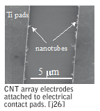 Injection of electrons and holes from the drain and source metal electrodes into the organic channel plays a key role in the performance of organic thin film transistors (OTFTs). Contacts between metals and organic semiconductors are generally non-ohmic because charge carriers have to overcome an energy barrier (Schottky barrier) at the interface, which significantly deteriorates the device performance thus limiting the capacity to scale-down the devices. A possible solution to this problem is to replace the metallic electrodes of OTFTs with carbon-based electrodes, such as carbon nanotubes (CNTs), i.e. rolled sheets of graphene in a seamless cylinder of diameter in the nanometer scale. CNT electrodes are gaining much momentum in the organic electronic community. Besides their high electrical and thermal conductivity, they offer properties that are highly desirable for applications in organic electronics, such as facile processing and printing, mechanical flexibility and chemical stability. The main motivations for the use of CNT electrodes in organic electronics are improving the injection of charge carriers and providing a replacement to metal electrodes in flexible carbon-based electronics.