
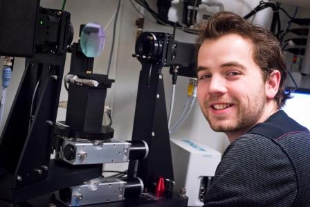
You will find, in this section, the complete list of all of our deposition and characterization equipement.

Various deposition and surface treatment systems are available in order to advance the research projects of our students and interns as well as contracts. Our main deposition techniques are:
|
 |
Please choose from the following list to obtain additional information:
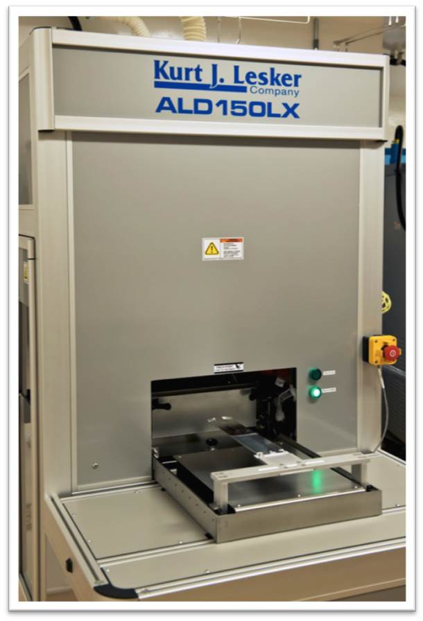
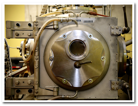
The ALD150LX is an ALD (Atomic Layer Deposition) system purchased from K.J. Lesker Company in 2013. The ALD technique relies on self-limiting sequential chemical reactions on the substrate surface in order to ensure film deposition with high conformity and thickness control on the atomic scale. In the ALD150LX, the sample is loaded through a rectangular port in the chamber and positioned in the reactant chamber where the deposition takes place. Up to four precursors or gas inputs are introduced through the top plate. A fifth input is available through the plasma port (not available yet).
Main features
- Default process: Al2O3 deposition (other processes and materials to be developped soon)
- Substrates from small irregular pieces up to 6 inch diameter wafers
- Real-time process monitoring (M2000 ellipsometer from J.A. Woollam)
- Top mounted vapor delivery
- Curtain gas flow design to minimize contamination on reactor walls and reduce unwanter side reactions
- Substrate heating up to 500°C
For more information
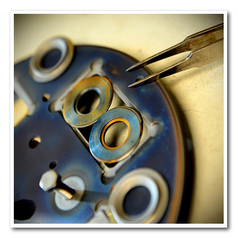
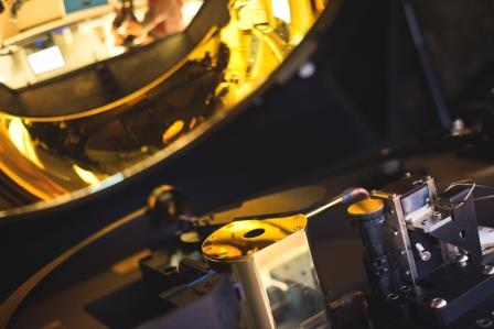
Our Dual Ion Beam Sputtering (DIBS) system is an industrial quality coating equipment which allows one to fabricate high-quality optical filters with an exceptional precision and uniformity. This apparatus is particularly suitable for demanding applications (e.g. telecommunications), and it allows a very fine control of the various deposition parameters. Thanks to the simultaneous use of two ions beams, it is possible to independently control the deposition rate and the structural properties of the layers.
Three interchangeable targets (1 ft diameter) can be installed on a target holder (e. g. tantalum, niobium and silica), offering to the user a large variety of materials. The metal targets make it possible to deposit metal or dielectric layers, while using appropriate gases, e.g. Ar, N2, O2. It is possible to mount up to nine 2”x 2” substrates in the deposition chamber. The whole system is computer controlled allowing for an almost complete automation of the process.
Several types of filters can be manufactured with this apparatus. Recent examples include, pass-band filters for astronomy, decorative filters, security devices, etc.
SYSTEM CHARACTERISTICS
- Materials: Nb, Nb2O5, SiO2, Ta, Ta2O5, Ti, TiO2 and others
- Rotating substrate holder (12” in diameter)
- Substrate temperature: 25 – 250 °C
- Ion sources: RF powered, 16 cm dia. for sputtering; 12 cm dia. for densification; hollow cathode neutralizers
- Ion energies: 0 – 1500 eV
- Gases: Ar, He, N2, O2
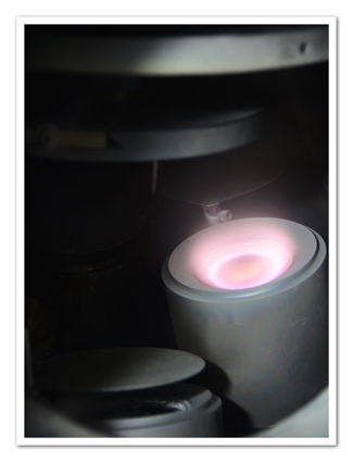
 High power impulse magnetron sputtering (HiPIMS or sometimes HPPMS) is a pulsed DC sputtering technique utilizing high power density peaks of typically more than 100 Wcm-2 at a sufficiently low time-averaged power density in order to avoid target overheating. This results in a high density discharge and, consequently, in a high degree of ionization of the sputtered material. This makes HiPIMS a very attractive deposition technique for enhancing and tailoring coating properties. For instance, a high number of metal ions in the deposition flux was found to be beneficial in substrate pretreatment for adhesion improvement, and in the fabrication of dense, defect-free coatings with low surface roughness.
Table 1: Typical discharge and plasma characteristics of HiPIMS and DCMS discharges.
| Cathode voltage | Peak Current density | Peak power density |
Peak Plasma density |
Ionization ratio |
|
| HiPIMS | 600 - 2000 V | 0.5-5 A/cm2 | 0.5-3 kW/cm2 | 1018 m-3 | up to 90% |
| DCMS | 300 - 700 V | < 0.1 A/cm2 | < 50 W/cm2 | 1015 m-3 | up to 1% |
Commercially available high power pulsed DC power supplies can be divided into two principal categories according to their respective power delivery in terms of pulse shape, voltage and current characteristics: (i) square voltage pulse generators allowing one to reach high cathode voltage values, which we label as HiPIMS PS, and (ii) custom-shaped voltage generators producing longer pulses of lower amplitude, applied for "modulated pulse power magnetron sputtering" (MPPMS). The representative pulse shapes and the instantaneous powers applied on the target, compared to DCMS power delivery (operated at the same average power P = 300 W), are schematically illustrated below.
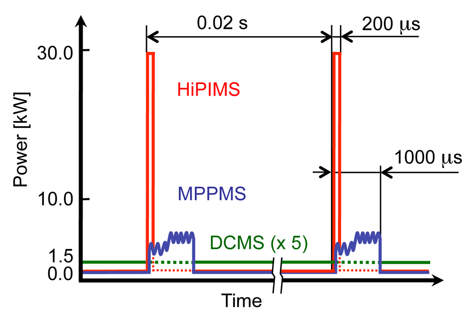
Figure 1: Pulse shapes and instantaneous applied power comparison for HiPIMS, MPPMs and DCMS power delivery systems.
The respective averaged optical emission spectra of HiPIMS, MPPMS and DCMS discharges are displayed in Fig. 2. It is visible that the HiPIMS spectrum is dominated by the most intense emission from Nb ions, indicating thus the highest ionization rate of the sputtered material.
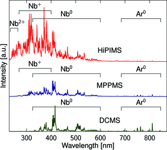
Figure 2: Averaged optical emission spectra of HiPIMS, MPPMS and DCMS discharges in argon over a Nb target.
Here, at the FCSEL, we apply several types of high power pulsed discharges (HiPIMS and MPPMS) in the deposition of metallic or dielectric films, using reactors of various sizes. These activities are complemented by in situ discharge monitoring by electrical and optical methods. Furthermore, we perform in-depth investigations of the gas-phase processes during the high power pulses, employing optical emission spectroscopy, plasma density analysis, mass spectrometry, and ion energy monitoring. This complex approach helps us to better understand and to optimize the discharge conditions necessary for a judicious control of the corresponding deposition processes.
Here are some characteristics of our deposition systems using the HiPIMS technique:
- Typically deposited materials: Cr, CrN, Ti, TiN, TiO2, Nb, Nb2O5, Ta2O5, SiO2, VO2, and others
- Deposition chamber sizes: 50 – 700 liters
- Magnetron sizes: 5-10 cm in diameter
- Gases: Ar, O2, N2
- Sample holders: 10-15 cm size in diameter, temperature range -20 °C to 400 °C, RF-induced negative biasing till ~ 1kV.
Below are the images visualizing the initial development of the HiPIMS discharge operated above a Cr target in different gases. The images were recorded through the viewing port by a high-speed ICCD camera. The time evolution is displayed above the image as "Time of discharge", that is a delay following the initiation of the voltage pulse.

More images and movies can be found in the following paper: M. Hala, N. Viau, O. Zabeida, J. E. Klemberg-Sapieha, L. Martinu, "Dynamics of reactive highpower impulse magnetron sputtering discharge studied by time- and space-resolved optical emission spectroscopy and fast imaging", J. Appl. Phys., 107 (2010) 043305.
For more information, please see the following papers related to our work on plasma imaging using band-pass interference filters (fabricated using our DIBS system):
- M. Hála, O. Zabeida, B. Baloukas, J. E. Klemberg-Sapieha, and L. Martinu. Time- and species-resolved plasma imaging as a new diagnostic approach for HiPIMS discharge characterization. IEEE Trans. Plasma Sci., 38(11) (2010) 3035-3039.
- M. Hala, O. Zabeida, J.E. Klemberg-Sapieha, L. Martinu, "Dynamics of HiPIMS Discharge Operated in Oxygen," IEEE Transactions on Plasma Science, 39 (2011) 2582-2583.
 We have developed, over time, different approaches for thin film and coating fabrication. The main characteristics of our PECVD systems are the following:
Microwave (2.45 GHz) plasma: Different applicators: slotted waveguide, slow-wave structure, and symmetric antenna.
Radio frequency (13.56 MHz) plasma: Capacitive coupling, control of the ion bombardment at substrate holder electrode.
Dual-mode MW/RF plasma: selective control of ion energy and ion flux.
Process gases: Ar, CH4, H2, HMDSO, O2, N2, NH3 SiCl4, SiH4, TiCl4, etc.
Pumping systems: mechanical rotary and turbomolecular pumps, corrosion resistant chemical pumps.
Sample holders: 10-20 cm diameters, temperature from –20 °C to 600 °C, RF induced negative biasing – till ~ 1kV.
Process control: Automated closed loop control; laser interferometry and reflectometry; real time in situspectroscopic ellipsometry; optical emission spectroscopy; mass spectrometry.
Studied materials: a-Si :H, DLC, Au/SiO2 nanocomposites (nc), TiN/SiN1.3-nc, TiCxNy/SiCN-nc, Si3N4, SiO2, SiOxNy, SixTiyO2, TiO2, etc.
The FCSE has acquired a lot of expertise throught collaboration with the industry such as the design of adapted reactors for deposition and treatment on various products. Here are a few examples:
- Control of ion bombardment, VUV, radical chemistry and (vacuum) ultraviolet radiation
- Powder treatment and coating
- 3D objects treatment and coating
- Hybrid PECVD/PVD systems, reactors for a selective control of plasma-surface interactions
- Fabrication of nanotubes, diamond, “plasma polymer”
- Continuous treatment of flexible webs, fibers and wires
 We also possess various sputtering systems with different configurations. Here are some of their most pertinent characteristics:
- Balanced magnetrons; diameters of 50, 75 and 100 mm
- Excitation mode: DC, pulsed DC (5 – 350 kHz), RF (13.56 MHz)
- Dual and quadrupal magnetron configurations
- Reactive and non-reactive sputtering
- Typically deposited materials: Al, Al2O3, Ag, Au, CrAlN, CrN, CrSiN, Cu, ITO, Nb2O5, SiO2, Ta2O5, Ti, TiO2, TiN, , TiSiCN, TiSiN, VO2, WO3, ZnO, etc.
 Developing new optical materials is part of our main research activities. As a result, we possess all the necessary equipement to obtain their main characteristics (transmission, reflection, absorption, colour, refractive index n and extinction coefficient k, thickness, etc.). Here is the complete list of our optical characterization equipement:
- Variable angle spectroscopic ellipsometer (VASE) RC2-XI J.A. Woollam Co., Inc.
- Spectroscopic ellipsometer M-2000UI J. A. Woollam Co., Inc.
Wavelength range: 210 nm - 2500 nm
Resolution: 1.6 nm (5 nm bandwidth) for wavelengths < 1000 nm
6.4 nm (12 nm bandwidth) for wavelengths > 1000 nm
Configuration: Rotating compensator - Spectroscopic ellipsometer M44 J. A. Woollam Co., Inc.
Wavelength range: 423nm - 764 nm
Resolution: 1.6 nm (5 nm bandwidth) for wavelengths < 1000 nm
6.4 nm (12 nm bandwidth) for wavelengths > 1000 nm
Configuration: compensateur rotatif - IR variable angle spectroscopic ellipsometer (IR-VASE) J.A. Woollam Co., Inc.
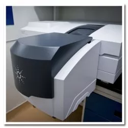
- Cary-7000 spectrophotometer with Universal Measurement Accessory (UMA)
- Perkin-Elmer Lambda 1050 spectrophotometer
- SOC-100 Hemispherical Directional Reflectometer
- Zeiss Axioscope A1 Optical Microscope
Ellipsometry is a non-intrusive optical characterization technique for deternining, among others, the thickness and optical properties [(n, k) or (ε1, ε2)] of thin films. The principle of this technique is based on the observation of the change in polarization state of a light beam after reflection on the surface of a sample. The fundamental equation of ellipsometry is:
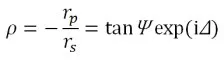
where rp and rs are the complex Fresnel coefficients corresponding to the thin film(s)-substrate system, and Ψ and Δ are the parameters measured by the ellipsometer, related to the amplitude and phase of rp and rsrespectively. After construction of a suitable optical model (substrate, number of layers, thickness and optical constants for each layer), the values of Ψ and Δ provided by the model are compared with the experimental values, and thourgh an iterative optimization process, the characteristics of the layers are determined. The measurement of the phase (Δ) is particularly sensitive to the thickness of the layers and can changes in the order of an angstrom can be detected. The refractive index can be obtained with an absolute accuracy of the order of 10-3 and a relative accuracy ≤ 10-4.
The RC2 ellipsometer is equipped with two rotating compensators which provide an excellent measurement accuracy (of the order of one hundredth of a degree on Ψ and Δ). This configuration also allows one to analyze samples that are both depolarizing and anisotropic. Note that additional modules can be installed on the RC2: XY mapping module, heating cell, electrochemicall cell, etc.
To learn more about ellipsometry: http://www.jawoollam.com/tutorial_1.html
RC2 CHARACTERISTICS
- Wavelength range: 210 to 2500 nm
- Resolution:
- Configuration: Dual rotating compensators
IR-VASE ellipsometry (Infrared Variable Angle Spectroscopic Ellipsometry) is a powerful non-destructive characterization technique combining the advantages of ellipsometry and infrared spectroscopy (Fourier Transform FTIRS). Thus, the thickness and optical constants (n, k) of multilayer coatings can be determined as well as the characteristic chemical bonds of the analyzed materials.
The determination of n and k allows one to overcome problems related to artifacts present on optical reflection spectra (peaks and interference due to the nature of the substrate, the thickness of the layer or the angle of incidence) and thus obtain the intrinsic properties of materials. The chemical sensitivity of the IR-VASE is greater than in the case of FTIRS, offering the possibility of detecting ultrathin layers (up to 5 nm) on many types of substrates. Finally, other film characteristics can determined such as: anisotropy, non-uniformity, LO and TO phonons and dopant concentration.
To learn more about ellipsometry: http://www.jawoollam.com/tutorial_1.html
IR-VASE CHARACTERISTICS
- Wavelength range: 333 cm-1 - 5000 cm-1 (2 micron - 30 microns)
- Resolution: 1 cm-1 - 128 cm-1
- Configuration: rotating compensator
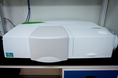 Spectrophotometry is a simple and versatile characterization technique with applications in variousareas: (i) Chemistry, to determine the concentration of a substance from a liquid absorbance spectrum using the Beer-Lambert's law (ii) in colorimetry, spectrophotometry is used to quantify the color of an object in agiven color space from a transmission or reflection spectrum, (iii) in the field of optical filters, the spectrophotometer evaluates the optical performance of filters in transmission or reflection, as well as otherparameters such as the thickness and the refractive index of the layers, as well as the absorption and scattering of materials.
CHARACTERISTICS OF THE PERKIN-ELMER LAMBDA 1050
- Wavelength range: 175 nm - 3300 nm (3 detector setup: PMT/InGaAs/PbS)
- Resolution: 0.05 nm - 5.00 nm (UV and visible)
0.2 nm - (NIR)
(8 absorbance units in sensitivity)
ACCESSORIES
Labsphere accessory for diffuse reflectance and transmittance
- Wavelength range: 250 nm - 2500 nm
- Angle of incidence: transmission: 0 degrees
reflection: 8 degrees - « Small Pot » module for a 1 x 1 mm focalized beam.
- « Light Trap » module to eliminate specular reflection.
 The FCSEL is the first laboratory in the world to be equipped with the Universal Measurement Accessory from Agilent Technologies! Installed on a Cary 7000 spectrophotometer this unique system allows one to measure both reflection and transmission at angles between 6° and 85° without requiring to move the sample manually; thus, contrary to other classical setups, the UMA ensures one that the same spot on the sample is probed as well as with the same beam characteristics. As a result, precise absorption measurements can now be performed. The angular selectivity of this setup also allows for scatterometry measurements to be performed in the case of diffusive samples.
For more information, please click here.
CHARACTERISTICS OF THE CARY-7000
- Wavelength range: 175 nm - 3300 nm (2 detectors : PMT/PbS)
- Resolution: 0.05 nm (UV and visible)
0.2 nm (NIR)
(8 absorbance units in sensitivity)
CHARACTERISTICS OF THE UMA SYSTEM
- Wavelength range: 250 nm - 2500 nm
- Angles of incidence: 0 to 85 degrees in transmission
6 to 85 degrees in reflection - Polarization control: s and p
 The SOC-100 HDR provides polarized, angular reflectance measurement from 10° to 80° incident angles. Coupled to the Nicolet 6700 FTIR, the SOC-100 HDR operates in the entire spectral region available for that FTIR. It provides the capabilities to measure the collimated and scattered transmittance of samples, and by using a specular beam blocker, the diffuse and specular partition of the scattered energy. From the direct measurements other values can be calculated: directional and near normal emissivity, directional angular emissivity, total hemispherical emissivity, solar absorptance, and optical constants (n and k).
Features
- Wavelength range: 1.5-25.0 μm (KBr beamsplitter) ou 1.8-45 μm (CsI beamsplitter)
- Detectors: 1.5-45 μm (DTGS) or 1.5-16.0 μm (N2 cooled MCT-A)
- Maximum spectral resolution: 0.09 cm-1
- Substrate-holder maximum temperature: 500°C
- Required sample size: 1” x 1”
Accessory
Smart SAGA (Specular Apertured Grazing Angle)
The Smart SAGA is ideal for grazing incidence analysis of sub-micron films on metallic substrates. Grazing angle reflectance is the technique of choice for analyzing thin coatings or deposits because the high angle of incidence increases pathlength of the infrared beam through the material of interest, significantly enhancing sensitivity. This accessory samples an average angle of 80 degrees from the normal. Analysis of films from 10 Angstroms to 0.5 microns is possible. A permanently mounted polarizer minimizes the ‘S’ polarized light which does not contribute to spectral data at the surface, increasing sensitivity and sampling speed. Samples are analyzed conveniently by placing them on a horizontal sampling surface and masked using a unique sliding aperture assembly.
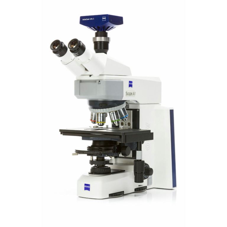 The Axioscope A1 is a modular microscope for research and routine material analysis.
Features:
- Bright field, dark field, phase contrast (DIC), polarized light modes in both reflection and transmission.
- LED source for reflection measurements, halogen source for transmission measurements
- 5 MP color camera for high resolution images
- Manual XYZ stage
- 5x, 10x, 20x EC Epiplan objectives
- 50x, 100x, EC Epiplan Apochromatic objectives
- Maximum sample height: 4 cm
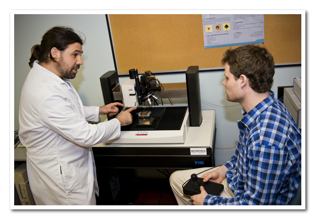
 Developing materials with specific mechanical properties is also one of our specialties (hardness, Young modulus, Poisson coefficient, adherence, erosion - corrosion - friction resistance, etc.). Here is a list of our characterization equipment
- Nanoindenter
- Microstratch tester
- Pin-On-Disc Setup
- Slip/peel tester
- Tencor FLX 2900
- High Load Tribometer
- In-situ Stress Measurements
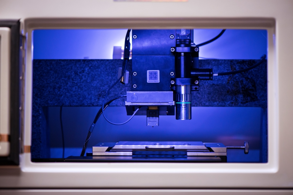 The Hysitron TriboIndenter® is an ultra-low load nanomechanical test system designed to measure the nanomechanical and nanotribological properties of thin films and material surfaces. From depth sensing indentation, one can measure the indentation depth, hardness, elastic modulus (Young's modulus), elastic recoverry, the wear resistance and scratch resistance. Surface imaging can also be performed.
FEATURES
- Applied load: 10 μN - 10 mN
- Load resolution: 1 nN
- Maximum depth: 20 microns
- Displacement resolution: 0.04 nm
- Thermal drift: <0.05 nm / sec
- Berkovich tip type
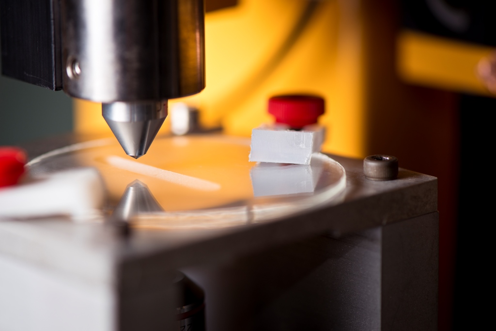
The microscratch tester (MST®) from CSEM, is used to characterize the surface as well as the micromechanical-microtribological properties of coatings and thin films, that is to say, the adhesion, hardness, coefficient of friction and resistance to wear. While perfomring a scratch on the surface of a sample using a Rockwell C diamondi-tip the MST measues the acoustic emission, the force normal to the sample, the frictional force as well as the depth of penetration. These measurements, combined with optical observations of the scratched surface, form a unique fingerprint of the studied layer/substrate system. The hardness can also be measured using a Vickets-type of indenter.
SYSTEM CHARACTERISTICS
- Charge: 0 to 30 N
- Rockwell C stylus radii : 50, 100 and 200 microns
- Scratch length: typically 5 to 15 mm
- Scratch speed: 0.01 to 16 mm / min
The pin-on-disc is an apparatus used to determine tribological properties of coatings. These properties include frictional coefficient and wear rate. The coated specimen is placed on a rotating disc spinning at a variable angular speed. A ball held by a vertically reciprocating pin is pressed against the sample for a fixed amount of full rotations of the disk. The tangential force and the frictional coefficient are measured and the volume of removed material can be measured by additional techniques.
SYSTEM CHARACTERISTICS
Monitored parameters:
- Frictional force
- Sliding speed u: 0.01- 0.5 m/s
- Load F = 0.3 - 50 N
Types of balls (3 and 6 mm radius) and their hardness:
- Al2O3 (15 GPa)
- HS steel (0.9 GPa)
- Sapphire (18 GPa)
- Si3N4 (17 GPa)
The Peel-Tester is an alternative test to the MST to measure the adhesive strength of thin films and coatings. An adhesive strip fixed to the coating is pulled at an increasing load (0 to 50 N) until bonding failure occurs. The type of failure that can be observed are cohesive, adhesive or substrate failure.
The same setup can also be used for the evolution of surface friction.
CONTROLLED PARAMETERS
Tangential force: 0 – 50 N
Temperature of the substrate holder: 0-200 °C.
The Tencor FLX 2900 is a thin-film stress measurement instrument. Specifically, the stress is obtained by comparing the change in radius of curvature of the substrate, with and without the film using the well known Stoney equation.The radius of curvature itself being obtained by simply measuring the angle of deflection of a laser beam off the surface of the substrate/sample.As a result, the substrate and/or the thin-film must be optically reflective at the measuring wavelength which is 670 nm in this case.
The Tencor FLX 2900 also offers the possibility to measure stress as a function of time or temperature in air or in a controlled atmosphere like nitrogen or argon.
The main characteristics of the instrument are the following:
Substrate size: 1”-8 “
Time measurements: 30 seconds to 300 hours
RMS noise: 0.0001 m-1 (radius 10 km)
Resolution: 0.00003 m-1
Minimum scan step: 0.02 mm
Maximum points per scan: 1250
Temperature range: 20- 900° C
Scan time: 5 s
Laser wavelength: 670 nm
Minimum radius: 2.0 m
Typical repeatability error (1σ):
|
Si<100> substrate thickness |
Film thickness |
|||
|
10 μm |
1 μm |
100 nm |
10 nm |
|
|
375 μm |
50 kPa |
0.5 MPa |
5 MPa |
50 MPa |
|
525 μm |
100 kPa |
1.0 MPa |
10 MPa |
100 MPa |
|
625 μm |
140 kPa |
1.4 MPa |
14 MPa |
140 MPa |
|
675 μm |
170 kPa |
1.7 MPa |
17 Mpa |
170 MPa |
The WINFLX softwareoffers adjustable recipes for thermo-cycling as well as for controlling the heating and cooling rates.
Additionally, by employing a two-substrate method , this instrument provides the possibility to determine the linear themal expansion coefficient of thin films. Additionally, in conjunction with nanoindentation measurements it also possible to measure the Poisson ratio [link to wiki?]. For more information on the application of the two-substrate method for different materials please check our paper entitled “Mechanical and Thermo-elastic Characteristics of Optical Thin Films Deposited by Dual Ion Beam Sputtering” [link]
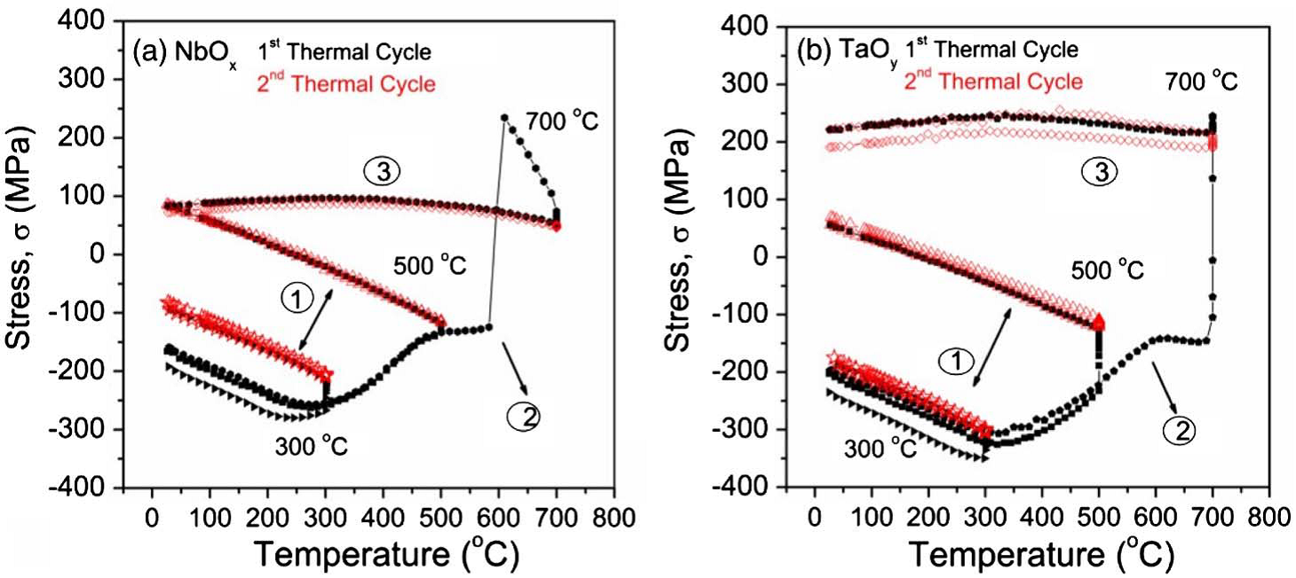
An example of the stress dynamics during thermocycling of niobium and tantalum oxide films is shown on the bottom figure.(This figure taken from E. Çetinörgü-Goldenberg, J. E. Klemberg-Sapieha, and L. Martinu, "Effect of postdeposition annealing on the structure,composition, and the mechanical and optical characteristics of niobium and tantalum oxide films", Applied Optics 51 (27 / 20) (2012) 6498-6507.)
The HLT500 is a tribometer devoted to wear studies at high normal loads. The system allows one to monitor classical tribological parameters (normal load, frictional force, normal displacement, rotational speed) and to perform tests in two different configurations.
The first configuration is related to the study of galling type of wear between two plane surfaces. In this mode, the samples have a cylindrical geometry with specific dimensions (ASTM G98 and G196). Note that other coupon sizes can also be adapted for such measurements. In order to prevent any misalignment between the two surfaces leading to an inhomogeneous contact pressure, the sample holder is equipped with an auto-alignment cell. The maximum normal load can reach 5000 N.
The second configuration is a standard pin-on-disk tribometer. Note that various ball sizes can be used to generate different contact pressures. The maximum normal load can reach 500 N. In both configurations, the system allows the generation different sliding motions (clockwise (CW) and counterclockwise(CCW)) and also allows on to work in a bidirectional cycling mode.
Table 1 - Main operation conditions
|
Configuration |
Galling |
Pin-on-Disk |
|
Normal load (N) |
20 - 5000 |
20 - 500 |
|
Auto-alignment cell |
Yes |
No |
|
Speed (RMP) |
300 |
300 |
|
Direction of sliding |
CW, CCW, bidirectional |
CW, CCW, bidirectional |
|
Output data |
Coefficient of friction (CoF), torque, displacement, speed, number of cycles |
CoF, torque, displacement, speed, number of cycles |
The k-Space Multi-beam Optical Sensor (kSA MOS) is a system used to determine the evolution of the stress/strain developed during the deposition of thin films.
The main principle behind the present stress measurements is based on the elastic deformation of the substrate-coating system during the deposition (using the well known Stoney approach). The technique uses an array of parallel laser beams to follow the evolution of the radius of curvature of a reflective substrate. Depending on the stress state (compressive or tensile), the laser array will undergo a convex or concavespatial deformation, which will translate into the laser spots getting farther apart (convex) or closer (concave) relative to each other. Fig. 1 show a schematic representation of our setup.
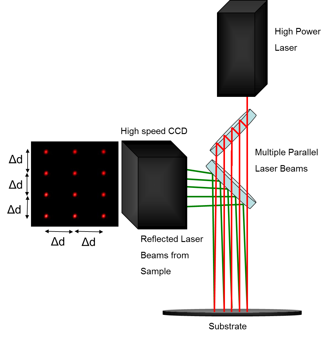
Fig 1: In situ stress measurement setup (kSA MOS)
The use of a laser enables to operate the system in any reactor or deposition chamber as well as in any environment (air, vacuum, plasma) or at any temperature. Moreover, the kSA MOS setup can also be used to assess the effect of surface treatment like ion bombardment or other transient phenomena, such as water adsorption during the venting stage.
 The 737 PC-Based Monitor (Delcom Instruments) is a surface conductivity characterization tool. The measurements are contactless and thus can be made without compromising the physical integrity of the sample; in contrast with the more typical 4-point-probe method, where the surface of the sample may need to be punctured in order to make contact with an underlying conductive film. As a result contactless sheet resistance measurements can easily probe buried conductive layers.
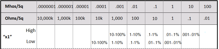
Present-day contactless measurement techniques are based on the interaction of a conducting layer submitted to a varying electromagnetic field. The most popular strategy is based on the induction of eddy currents in the conductive layer using an alternating magnetic field (Krupka, 2013). In this setup, the magnetic field is generated across the conductive sample thus inducing eddy currents which in turn will generate an opposing magnetic field; this effect is then quantified and converted into sheet resistance (Miller et al., 1976). In fact, the power which is absorbed in the production of eddy currents at a particular frequency is proportional to the conductivity of the thin film (note that the thickness of the conductive material must be less than the skin depth). Thus, by calibrating with a test material with a known thickness and conductivity, it becomes possible to test layers with different conductivities. The measurement range and precision of our system are given in the following table:
Table 1: Measurement range and precision of our contactless sheet resistance setup. From Delcom 737 instrument manual.
A schematic representation of a contactless sheet measurement apparatus is displayed in Figure 1.
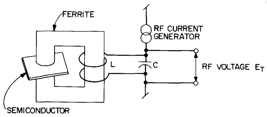
Figure 1: Contactless sheet resistivity measurement setup. From Miller et al., 1976
The PGSTAT302N potentiostat/galvanostat from Metrohm Autolab BV allows the complete electrochemical characterization of materials through the use of various techniques; constant voltage (potentiostatic), constant current (galvanostatic), potential varying in time (e.g.: cyclic voltammatry), etc. The additional FRA32M module also allows for electrochemical impedance spectroscopy.
Technical specifications of the PGSTAT302N
- Potential range : -10 V à 10 V
- Maximum current : -2 A à 2 A
- Current ranges : 10 nA à 1 A
- Potential resolution : 3 μV
- Current resolution: 0.0003 % of current range
- Computer interface : USB
- Control software : NOVA 1.10
Application examples
By employing a standard three-electrode setup, one can, for example, measure the resistance to corrosion of a material by using potentiostatic and potentiodynamic polarisation techniques. Such measurements allow the quantification of the effect of a passivation layer, the measurement of the floating potential and corrosion currents, etc.
A three-electrode setup can also be used in order to characterize active materials. For example, electrochromic materials (EC) such as WO¬3, NiO, V2O5 and other semi-conductor oxides see their optical properties change upon the combined insertion of electrons and ions. The bottom figure shows the classic "duck-shape" of a cyclic voltammogram obtained for an amorphous WO3 film; a material which is heavily studied at the FCSEL (see article by B. Baloukas et al.). By analyzing such a curve, one can determine the diffusion coefficient of ions in the film, the ratio of extracted to inserted charges, the anodic and cathodic currents, observe the presence of secondary reactions, etc. In addition, by combining such a measurement with in situ transmission, it is possible to calculate the coloration efficiency of the material, i.e. its variation in transmission as a function of inserted charge. Finally, by installing an electrochemical cell on our RC2 ellipsometer, it is also possible to obtain the intrinsic optical properties of EC materials at different stages of intercalation as a function of time. Providing many advantages/possibilities, this technique can be of interest for quantifying a material's durability/cyclability (see the article by H. Camirand et al.).
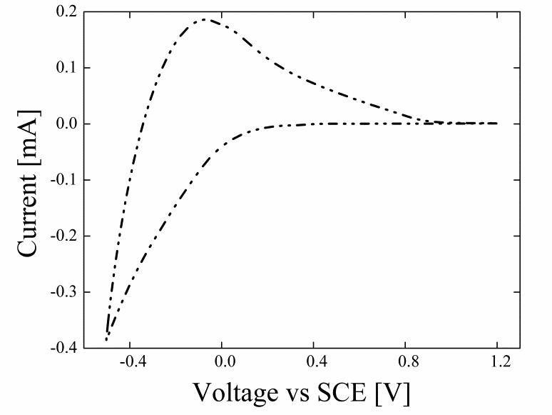
Figure 1 : Cyclic voltammogram of a 150 nm thick amorphous WO3 film deposited by reactive RF magnetron sputtering at a pressure of 20 mTorr (2.67 Pa). Measurement perfomed in a 0.1 M H2SO4 electrolyte using a saturated calomel reference electrode (SCE).
Energy resolved mass spectrometry is an advanced analysis technique of the physico-chemical profile of gases. This technique is based on the separation of charged particles according to their respective energy and their m/z ratio (mass to charge ratio). Note that neutral species can also be ionised at the entry of the spectrometer by electronic bombardment.
In the context of plasma diagnostics, mass spectrometry may be implemented in three 3 analysis modes : RGA (residual gas analysis) for analysis of neutral particles, SIMS+ and SIMS- (Secondary Ion Mass Spectrometry) for the analysis of the energy of positively and negatively charged particles. This then allows one to obtain the composition of the plasma and the energetic distribution of the ions arriving on the exposed surface. Furthermore, the instrument can produce time resolved measurements in order to evaluate the dynamics of the neutral and charged species. This approach is particularly of interest for the analysis of pulsed discharges. (For an example, please consult the article : O. Zabeida, A. Hallil, M. R. Wertheimer, and L. Martinu, "Time Resolved Measurements of Ion Energy Distributions in Dual-mode Pulsed Microwave/Radiofrequency Plasma", J. Appl. Phys., 88 (2000) 635.)
TECHNICAL SPECIFICATIONS
Mass spectrometer EQP-1000 by Hiden Analytical :
- Quadripole mass analyser, 0.2 to 500 amu.
- Energy analyzer up to 1000 ev.
- Electron multiplier detector : up to 107 c/s.
Differential pumping chamber :
- Working pressure 0-50 mTorr (100 µm extractor) or 50-300 mTorr (50 µm extractor)
- Extraction between polarizable electrodes (RF or DC)
- Plasma analysis (Sputtering and capacitive discharge)
- Fragmentation study (RGA or capacitive plasma)
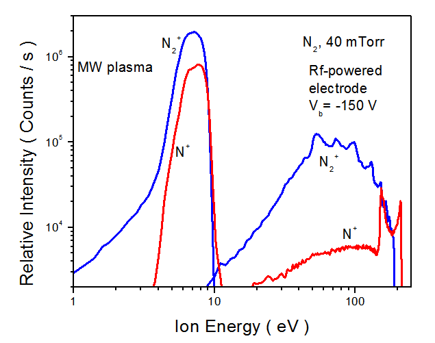
Figure 1: Example of the energy distribution of N2+ and N+ ions from a micro-wave plasma (left) and radio-frequency (right) is shown. N+ ions suffer fewer collisions in the sheath; this increases their average energy which is therefore higher than the average energy of the N2+ ions. Image taken from : A. Hallil, O. Zabeida, M.R. Wertheimer, and L. Martinu, "Mass-resolved Ion Energy Distributions in Continuous Dual Mode Microwave/Radiofrequency Plasmas in Argon and Nitrogen", J. Vac. Sci. Technol A, 18 (2000) 882-890.
Optical emission spectroscopy is a non-intrusive and non-disturbing plasma characterisation technique. It relies on the detection of photons which are emitted during the deexcitation of the energetic particles in the plasma. Since the times associated with deexcitation energy transitions are very short , it is possible to obtain time-resolved measurements down to the nanosecond when using equipment with a sufficiently high sensitivity.
ADDITIONAL DETAILS
When using optical emission spectroscopy, the light produced by the particles is collected by optical devices, such as an optical fibre or a collimator, and directed to a spectrophotometer. The scanned volume is then equal to the "perceived" space in direct view of the optical device. For example, in the particular case of an optical fiber, which possesses a small numerical aperture, the scanned volume is of only a few µm³. The collected light is then separated into its constituent wavelengths typically by using a diffracting grating.
The intensity of the diffracted light is then evaluated by a detector, either a CCD analyser or a photomultiplier. CCD analysers have the advantage of measuring multiple wavelengths at the same time, but possess a fixed intensity contrast. In opposition, photomultipliers measure a single wavelength at a time, but possess a far better contrast simply by adjusting the collected intensity.
The data obtained by optical emission spectroscopy contains a large amount of information. Every optical transition is precisely characterised by allowed-electronic transitions to which are also added the vibration energies of polyatomic particles. The position of each spectrum line therefore gives important information on the chemical composition of the plasma whereas their relative intensity informs us on the energy distribution between the various species in the plasma.
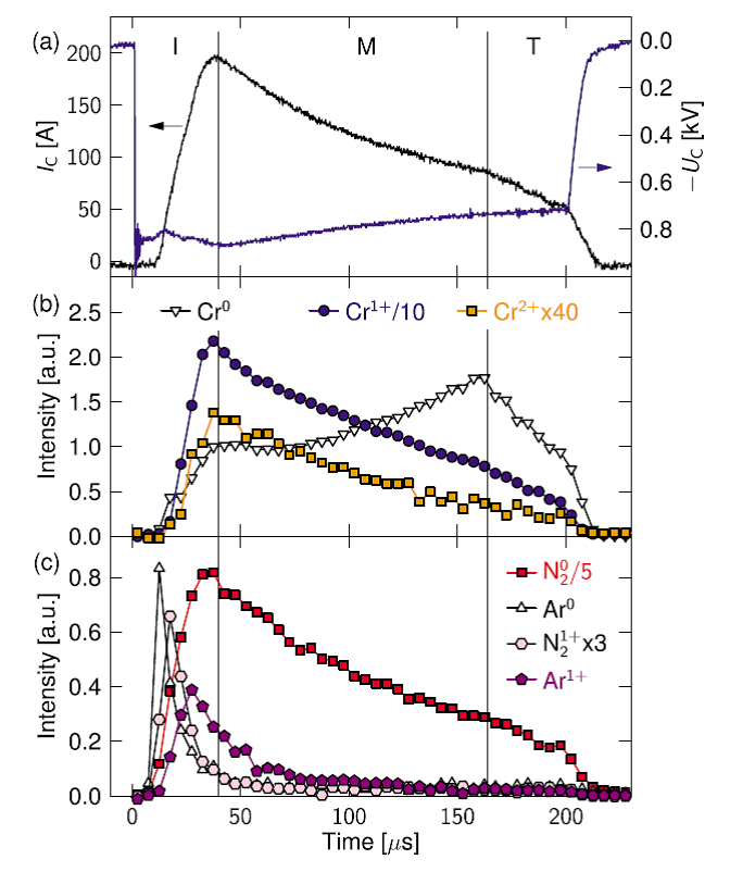
Fig.1 Temporal evolution of a HiPIMS discharge with a cathode voltage of -900V over a chromium target in a gas mixture of N2 and Ar of (1:1 ratio) at 1.3 Pa. The three development phases of the plasma are shown : the plasma ignition phase, the phase dominated by metallic emission and the transition phase to a DC-like discharge. (a) current and voltage of the discharge (b) emission intensity of the chromium ions (c) emission intensity of the gas species.
SPECIFICATIONS OF THE SPECTROMETER ACTON SPECTRA PRO
- Wavelength range : 200 nm – 1050 nm (3 gratings :120/1200UV/2400)
- Resolution: 0.393 nm @ 763 nm (120g), 0.033 nm @ 763 nm (1200g) and 0.017 nm @ 440 nm (2400g
- Detector : CCD amplified Pi-MAX II, 1024x1024 pixels over 16 bits (Max contrast 65535:1)
- Temporal resolution of the CCD : 5 ns
- Synchronisation delay : 150 ps- ms
SPECIFICATIONS OF THE SPECTROMETER OCEAN OPTICS USB2000
- Wavelength range: 170 nm - 870 nm (fixed grating :600)
- Resolution: 1.5 nm
- Detector: Linear CCD 2048 pixels (Max contrast 1300:1)
- Temporal resolution: 1 ms
- No synchronisation available
SPECIFICATIONS OF THE SPECTROMETER OCEAN OPTICS HR4000
- Wavelength range: 340 nm - 780 nm (fixed grating :600)
- Resolution: 1.5-2.3 nm
- Detector: Linear CCD 3648 pixels (Max contrast 1300:1)
- Temporal resolution: 3.8 ms
- No synchronisation available
Consult our HiPIMS section for more emission spectra examples.
Plasma imaging using a high speed camera is a complementary analysis technique to optical emission spectroscopy. With the help of an amplified CCD with a high shutter speed, it is possible to follow the dynamics of light radiating from excited species inside the plasma as a function of time as well as at different positions inside the reactor (time- and space-resolved). Note that the fairly recent improvements in the last decade of amplifying coatings and of CCD cameras has allowed large increases in spatial and temporal resolution.
At the FCSEL, we have also implemented energy-resolved measurements by using band-pass interference filters, specially designed and deposited using our DIBS, to separate the emission lines of the neutralgas species (argon, oxygen in the 750-900 nm range) from the ionised and metallic species in the plasma (400-450 nm range). For an example, please consult our following article : M. Hala, N. Viau, O. Zabeida, J. E. Klemberg-Sapieha, L. Martinu, Dynamics of reactive high power impulse magnetron sputtering discharge studied by time- and space-resolved optical emission spectroscopy and fast imaging", J. Appl. Phys., 107 (2010) 043305-1-9.
SPECIFICATIONS OF THE SPECTROMETER ACTON SPECTRA PRO
Princeton Instruments Pi-Max:1300 with photo-sensibilitator Unigen II :
CCD sensor : 1250x1250 pixels.
Wavelength range : 150-900 nm
Image acquisition speed : 0.6 images per secondes.
Temporal resolution : < 7 ns.
Minimum delay generator : 10 ns to 21 s.
Plasma diagnostics using a Langmuir probe allows the measurement of useful plasma parameters such as the electronic temperature, the electronic and ionic density, the electron energy distribution and the plasma potential. The method itself is based on the measurement of the current going through an electrostatic probe inserted in the plasma as a function of the applied potential. Modeling of the sheath's behaviour as a function of the potential drop, proposed by Irving Langmuir, allows the extraction of the plasma parameters.
The ESPion system from Hiden Analytical automates the data acquisition by allowing a programmable potential ramp and a motorised axial displacement. It is then possible to measure the dynamic and spatial variations of the plasma inside the chamber. The analysis of the data can be done using the ESPionSoft software or analytically in the case of plasmas which deviate from the optimal measuring conditions. Modeling of the behaviour of the Debye sheath depends on the surface state of the probe and of the behaviour of the electrons inside the plasma. It is therefore difficult to apply this analysis in systems where the surface conditions of the probe or the dynamic range of measurements vary faster than the acquisition rate (surface modification of the probe or magnetic fields)
SPECIFICATIONS OF THE ESPION SYSTEM
Controller:
- Voltage : -200 V to +100 V
- Current : 20 µA to 1 A formatted in 12 bits (4095)
- Acquisition rate : 69000 points/s
- Maximum acquisition frequency : 1 MHz
- Possible synchronisation for time resolved measurements
Probe :
- Length: 10 mm.
- Diameter: 0.15 mm.
- Materials : Tungsten, tantalum or molybdenum
- Displacement: 60 cm.